The broad image sensor portfolio provides options for camera manufacturers to satisfy the requirements of every possible end application from wearables and consumer electronics to demanding industrial and automotive applications. These image sensors enable flexibility in configuration and combine optimal performance characteristics, such as high speed, high sensitivity, and high image quality to match specific application requirements. They also provide an easy upgrade path for existing customers and allow manufacturers to leverage a single camera design to support multiple products to accelerate time to market.
Products By Megapixels
Image Sensors - 0.3 to 1 MP
Product family of high performance sensors ranging from 0.3 to 1 megapixels.
Image Sensors - 1.2 to 5 MP
Product family of high performance sensors ranging from 1.2 to 5 megapixels.
Image Sensors - 5.1 to 10 MP
Product family of high performance sensors ranging from 5.1 to 10 megapixels.
Image Sensors - 10.8 to 45 MP
Product family of high performance sensors ranging from 10.8 to 45 megapixels.
Products By Frame Rate
Image Sensors - 4 to 30 fps
Product family of high performance sensors ranging from 4 to 30 fps.
Image Sensors - 31 to 92 fps
Product family of high performance sensors ranging from 31 to 92 fps.
Image Sensors - 100 to 815 fps
Product family of high performance sensors ranging from 100 to 815 fps.
Featured New Products
View All Products

Related Resources
Technical Paper
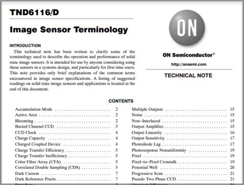
Image Sensor Terminology
This technical note has been written to clarify some of the terminology used to describe the operation and performance of solid state image sensors. It is intended for use by anyone considering using these sensors in a systems design, and particularly for first time users. This note provides only brief explanations of the common terms encountered in image sensor specifications.
Technical Paper
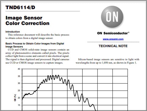
Image Sensor Color Correction
This reference document will describe the basic process to obtain colors from a digital image sensor. CCD and CMOS solid-state image sensors contain an array of photosensitive elements called pixels. The pixels collect light from a scene and convert it into electrical signal. The signal is then digitized and processed. Digital cameras use CCD or CMOS image sensors to capture images.
Application Note
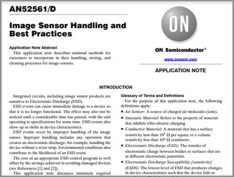
Image Sensor Handling and Best Practices
This application note describes minimal methods for customers to incorporate in their handling, storing, and cleaning processes for image sensors. Integrated circuits, including image sensor products are sensitive to Electrostatic Discharge (ESD). This application note discusses minimum required procedures to minimize the occurrence of an ESD event when handling image sensors.
Application Note
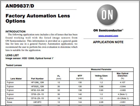
Factory Automation Lens Options
The following application note includes a list of lenses that has been found working well with the listed image sensors from ON Semiconductor. This information is provided as a general guide line for lens use in a general Factory Automation application; we recommend the user to perform his own evaluation to determine which lens is suitable for the application.
Application Note
X-Cube Imaging System X-Cube Machine Vision Reference Module Developer Guide
This document describes both the mechanical and electrical features and functions of the X−Cube Imaging System (X−Cube). The X−Cube is designed to demonstrate the features of ON Semiconductor’s XGS family of image sensors in machine vision applications. The X−Cube is designed to conform to the machine vision industry standard 29 mm × 29 mm form factor.
Application Note
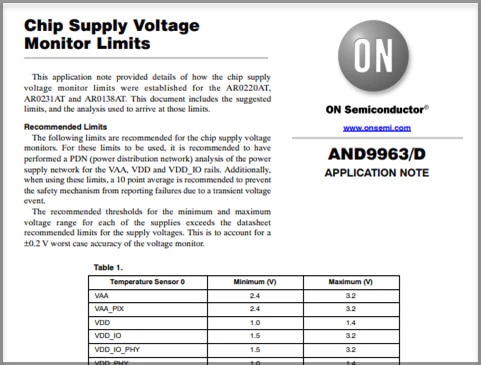
Chip Supply Voltage Monitor Limits
This application note provided details of how the chip supply voltage monitor limits were established for the AR0220AT, AR0231AT and AR0138AT. This document includes the suggested limits, and the analysis used to arrive at those limits.