Modern automotive, industrial, and datacenter systems are pushing deeper into the 48–90V domain. Designers need higher voltage, tighter isolation, and mixed-signal integration but traditional BCD and SOI approaches force painful trade-offs: thermal limits, area penalties, parasitic coupling, or cost.
The high voltage Treo Platform is onsemi’s primary technology for covering all applications above 45V. It integrates selectable 45V, 70V and 90V DMOS modules with low-voltage CMOS in ±90V deep trench isolation. The platform is highly suited for complex driver and power supply designs targeting automotive, industrial or datacenter power applications up to 90V. The 70V and 90V devices are well tuned to common 48V supply domain requirements.
To address these system-level demands without the usual penalties of conventional HV integration, the high voltage Treo platform is built on an isolation concept that combines strong electrical decoupling with efficient monolithic integration. In this way, Treo HV combines SOI-like design freedom with the cost efficiency and thermal advantages of a bulk-silicon substrate.
±90V “Quasi-SOI” Isolation Architecture
Treo high voltage adopts the proprietary high‑voltage deep-trench isolation architecture originally developed and validated in onsemi’s predecessor 180nm BCD technology.
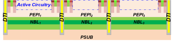
The isolation scheme (Fig. 1) consists of isolated P-type islands – so-called pockets – that are laterally isolated from neighboring pockets by deep trench isolation (DTI), and vertically isolated from the highly doped P-substrate by an intermediate N-type buried layer (NBL). Each pocket features symmetric ±90V isolation relative to the underlying substrate, enabling ±90V common mode operation on the P-epi. Within the ±90V operating range, the NBL provides behavior comparable to the buried oxide (BOX) of SOI technology, while offering much better thermal conductivity:
- The large headroom and lack of direct clamping/rectification effects allow for excellent handling of large transients and/or EMC disturbances.
- Pocket-to-pocket couplings and the bipolar parasitics are highly attenuated, providing immunity against latch-up.
- All devices support a common mode level of ±90V relative to the substrate
Treo high voltage’s isolation therefore enhances functional independence between circuit domains (e.g. tolerance to ground loss, reverse currents, etc.), enabling reliable operation in harsh environments and facilitating ISO26262-compliant system design.
Treo high voltage’s isolation therefore enhances functional independence between circuit domains (e.g. tolerance to ground loss, reverse currents, etc.), enabling reliable operation in harsh environments and facilitating ISO26262-compliant system design. At the system level, this translates into greater freedom to partition circuit functions and manage multiple voltage domains without compromising robustness.
Compact Intra-pocket Isolation
While pocket-level isolation enables robust separation between circuit domains, high integration density also depends on how efficiently devices can coexist within each isolated region.
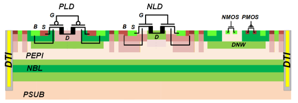
Within a single P-epi pocket, low‑voltage CMOS and high‑voltage lateral DMOS (NLD,PLD) devices can coexist (Fig. 2), provided their body potentials differ by no more than 6V.
Compact isolation is realized by confining the high voltage drains of the NLD and PLD devices to the internal device region.
Devices can be placed directly adjacent to the DTI boundary, yielding a pocket footprint comparable to that of high-voltage SOI technologies.
Deep N‑well (DNW) islands enable local isolation of CMOS devices, supporting voltage domains up to 3V, 6V and 24V versus the P-epi.
All Treo low voltage devices, libraries and circuit IP are supported in Treo high voltage, including the 1.2V 65nm CMOS option. The HV platform also retains full compatibility with all ≤24V Treo MV modules; low Rsp 6V and 12-24V DMOS options can be integrated into any Treo HV design. This implies that bootstrap voltages up to 24V above 90V (i.e. 114V) are supported without stressing the HV isolation.
Treo High Voltage Device Portfolio
Built on this isolation architecture and compact integration scheme, the device portfolio gives designers the flexibility to optimize voltage capability, area efficiency, and functionality at the product level. This breadth is what allows designers to tailor conduction, robustness, and integration to the exact needs of automotive, industrial, and datacenter systems.
In addition to the standard availability of all Treo low voltage and MV (≤24V) devices, the technology comprises several high-voltage device classes – NLD, PLD, diodes and passives – each implemented across three voltage families: 45V, 70V and 90V, respectively. The voltage level of each family refers to the rated (DC) operating voltage. Scaled 30V and 60V variants provide improved area efficiency at slightly lower VDS ratings. All DMOS devices share the same 2.5V gate oxide used in the Treo LV CMOS platform.
Within each DMOS voltage family, dedicated drain implants and a double RESURF architecture enable an optimal trade-off between specific on-resistance (Rsp) and breakdown voltage (BVDSS). This gives circuit designers the flexibility to match device flavor and voltage class to the exact conduction, robustness, and integration needs of the end application.
Two device flavors are available; both are using the exact same layers but are optimized for either switching (lowest Rsp) or analog operation (robustness under continuous high-VDS current). Both static (BVDSS and BVON) and dynamic (VT1) breakdown voltages provide sufficient margin to ensure robustness under the most demanding operating conditions. All device models are validated over a temperature range from −40°C up to +200°C. HV switches, diodes and pockets include full parasitic modeling down to the P-substrate.
- The device portfolio is complemented by high voltage passives, including
Poly resistors (up to 3kΩ/□) on top of the STI isolation
- Metal-Metal finger capacitors are available across all metal levels of the selected metal stack, with voltage ratings ranging from 45V up to 90V, available. Capacitor slices can be stacked on top of existing IP, enabling area-efficient integration.
High Voltage Device Construction
To see how Treo high voltage delivers this combination of voltage range, compactness, and robustness, it is useful to look at the construction of its key high-voltage devices.
NLD devices (Figure 2, middle) implemented within the same pocket always share a common P‑epi body. Unlike N-epi based technologies, the NLD drain is electrically decoupled from the underlying NBL isolation. This leads to a reduction in drain capacitance and mitigates noise injection into the substrate. Alongside standard enhancement-mode NLD devices, also depletion-mode versions are available as an option.
The PLD (Fig. 2, left) is realized as a closed N-resurf structure, where the P-type drain region is fully enclosed by the N‑type body and therefore isolated from the underlying P-epi.
This construction enables multiple independent PLD devices to share the same pocket; PLD bodies can remain independent or abutted.
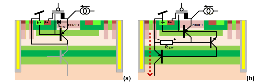
In case of a stand-alone PLD (Fig. 3), the majority of the parasitic injection (e.g. during body diode conduction) is captured in the local P epi (Fig. 3a), while the underlying NBL suppresses propagation into the substrate (Fig. 3b).
Together, the NLD and PLD options provide complementary building blocks for integrating efficient power devices alongside sensitive analog and interface circuitry.
For the same reason, the closed resurf HV diodes – which are based on the corresponding PLD – feature low injection into the substrate. In addition, their terminals can swing ±90V versus substrate, independent of the operating mode (forward or reverse). The absence of clamping effects makes these diodes well-suited for building the EMC-immune ESD networks for the input pins of advanced sensor interfaces and in-vehicle-network (CAN/LIN/Ethernet) transceivers.
These device-level properties reinforce the broader platform value introduced at the beginning: Treo high voltage is not only about reaching higher voltage, but about doing so with the isolation quality and functional robustness needed for demanding mixed-signal systems.
Summary
Treo high voltage is onsemi’s new high-voltage platform, compactly co-integrating 45V, 70V and 90V DMOS devices with low-voltage CMOS in a ±90V deep trench isolation architecture. The broad high voltage device portfolio, compatible with Treo LV and Treo MV (≤24V) modules, enable efficient mixed‑signal designs for the most demanding automotive, industrial and cloud applications. Typical applications include E-fuses, E-fuse controllers, BLDC motor controllers, gate drivers, ethernet transceivers, DC-DC converters, among others. The high voltage Treo Platform provides a scalable, future‑ready foundation for the next wave of innovation in power management, motor control, sensing, and connectivity.
Learn more about the Treo Platform